Cârpino's circuit design#
The whole Cârpino board's design was made in KiCad 7.0 (open-source software).
The design is made open and is fully explained in this article. Screenshots will be provided along with short descriptions.
The schematic#
For those interested to see the final Cârpino board, here is the complete schematic:
An overview of the whole schematic of Cârpino (the second revision)
In the following paragraphs, I will break down the most important parts of the circuit so that the overview above makes more sense.
The power supply#
Considering an input voltage VCC, we want to get a 5V output. To do so, we can use the NCP718 voltage regulator, which will reliably output the requested voltage, as long as VCC is high enough.
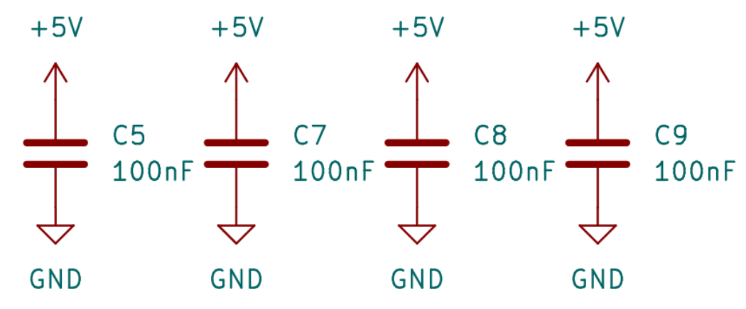
A few capacitors should be used as well in order to reduce noise.
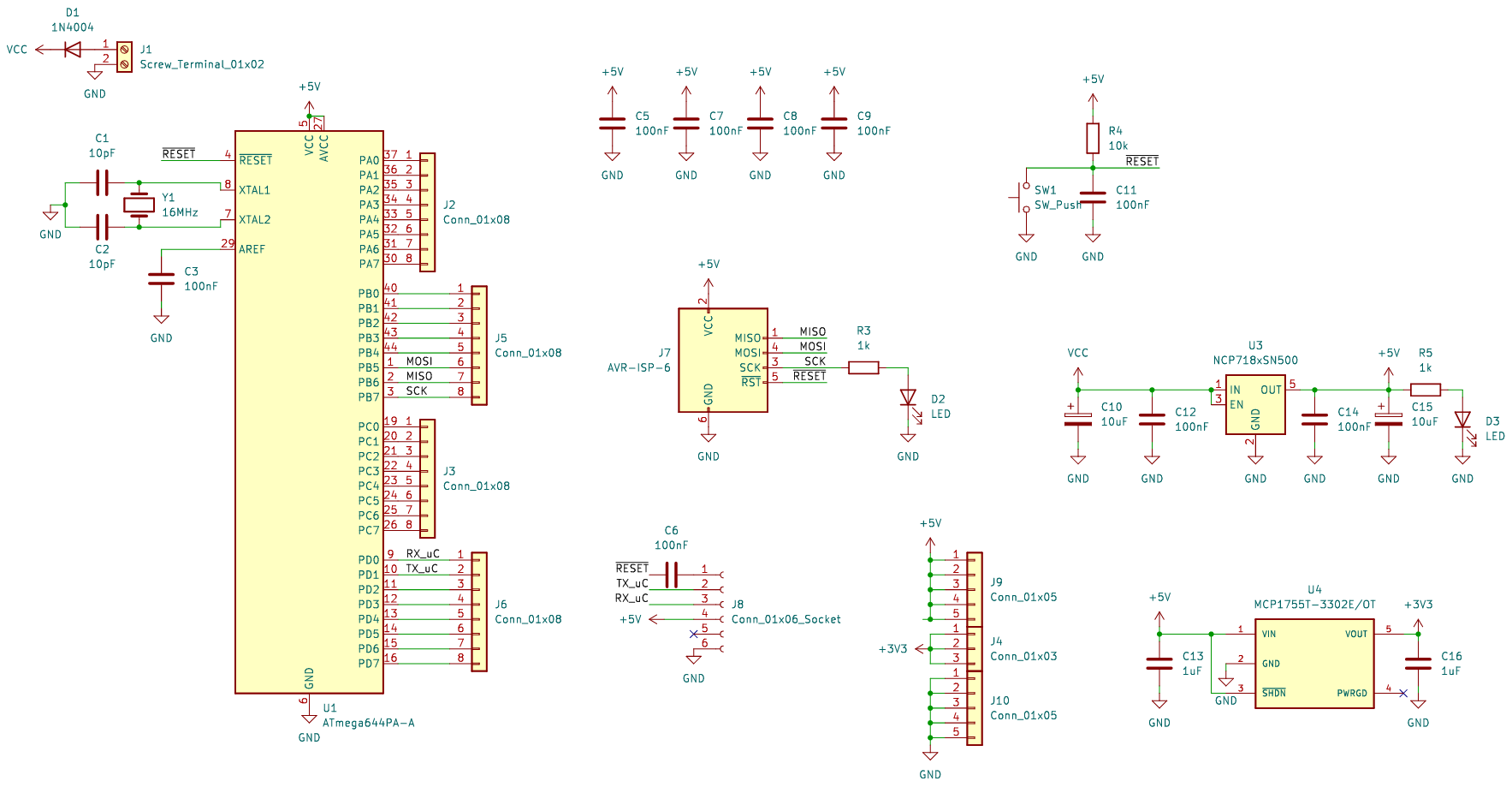
The VCC input
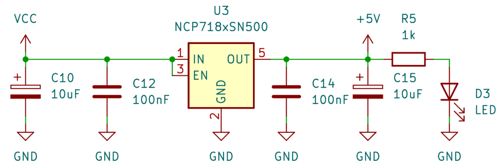
The 5V regulated output
It is also possible to power the board directly through the UART interface. In that case, no voltage regulation is required to get 5V.
It goes without saying that, whenever a 5V input is required, a decoupling capacitor should be used as well:
The 5V regulated output
To get 3.3V, we need to choose whether to convert VCC or 5V. However, since we don't always get VCC (due to UART), we will convert the 5V.
Please note that the MCP1755 was used only because that was what I've had lying around at that moment - NCP718 can be used as well.
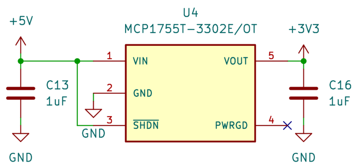
The 3.3V regulated output
The 16MHz clock#
A 16MHz crystal oscillator was used to generate the fixed clock frequency. As a design consideration, the crystal will be placed in close proximity to the ATmega644PA chip.
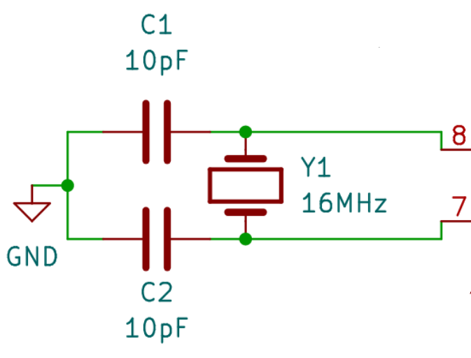
The 16MHz connection
The AVR interface#
The AVR interface requires 6 pins: a voltage input (5V), a ground pin (GND), a reset signal (\(\overline{\text{RESET}}\), active on 0), MISO, MOSI and SCK.
More details can be found here. In theory, once the basic configuration is flashed on the chip, these pins should become unnecessary.
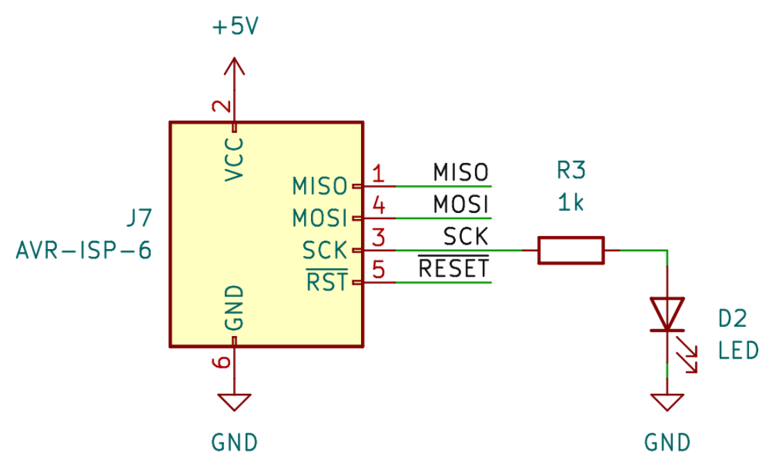
The AVR interface
The MISO, MOSI, SCK and \(\overline{\text{RESET}}\) pins should be directly connected, in this order, to the following ATmega644PA pins: PB6, PB5, PB7 and \(\overline{\text{RESET}}\).
The UART interface#
In order to communicate via USB, an UART connection has to be established first. To do so, we will simply expose some of the ATmega644PA's pins to a pin header.
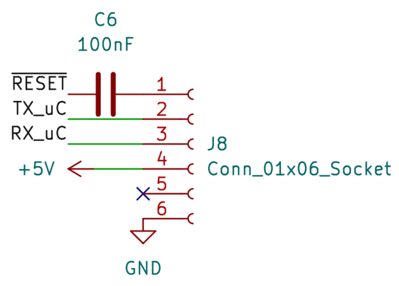
The UART interface
The RESET button#
Finally, a button can be used to manually reset the microcontroller:
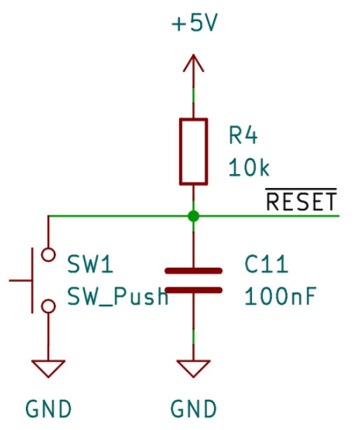
The reset button
The rest of the schematic#
The only thing left to do is to expose the rest of the pins that the microcontroller offers via pins/pin headers.
Selecting the components#
The real-world components need to be selected now. This is a simple process, but it requires trial and error and some experience.
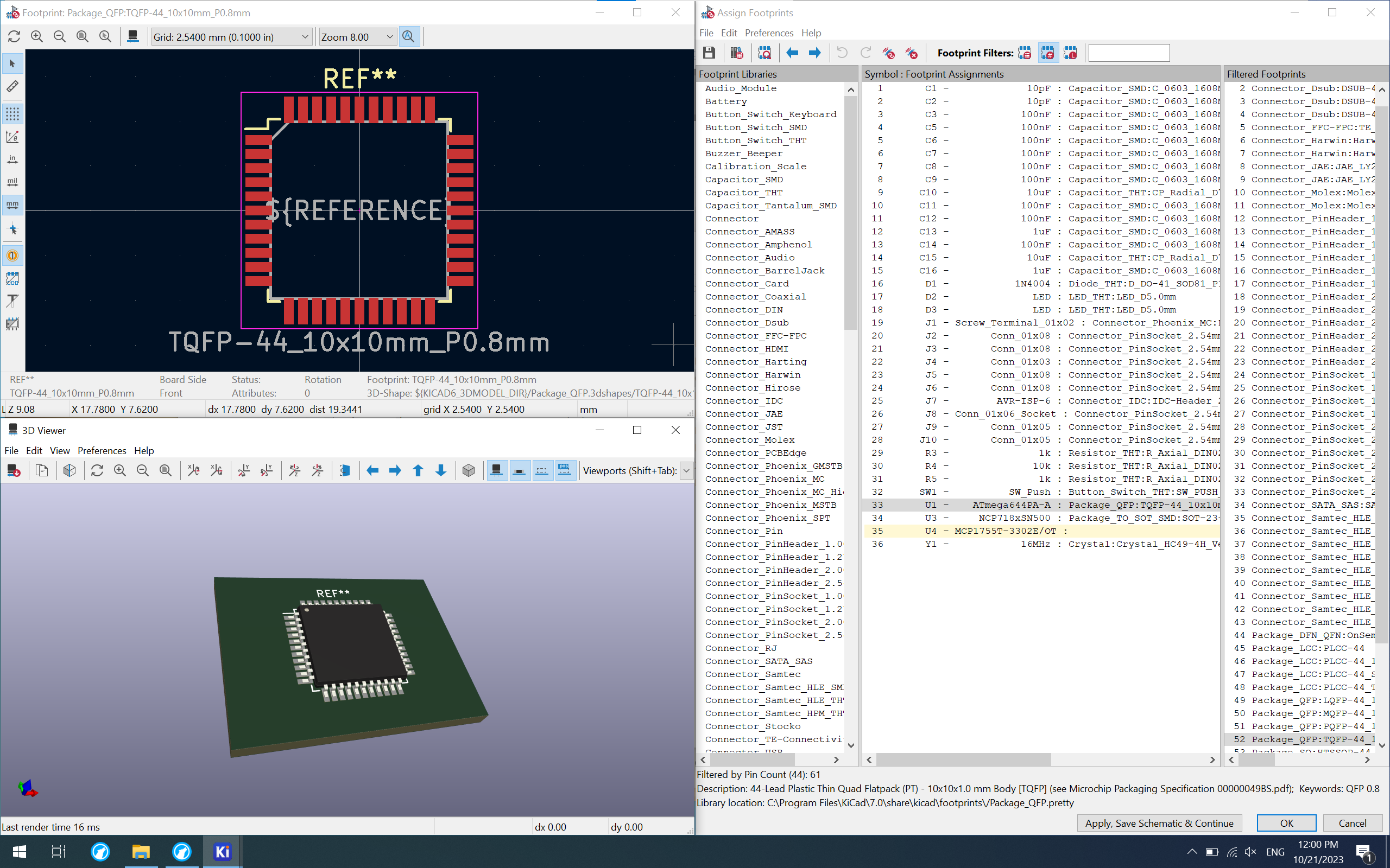
The component choice
You can find a bill of materials attached here.
The PCB#
Once everything else is ready, the PCB design process begins - this took me a while, since I wanted it to be neat, simple, and only require cooper routes on the back side.
Yes, I ended up with a small cooper route on the front side, but the final result is really beautifully crafted:
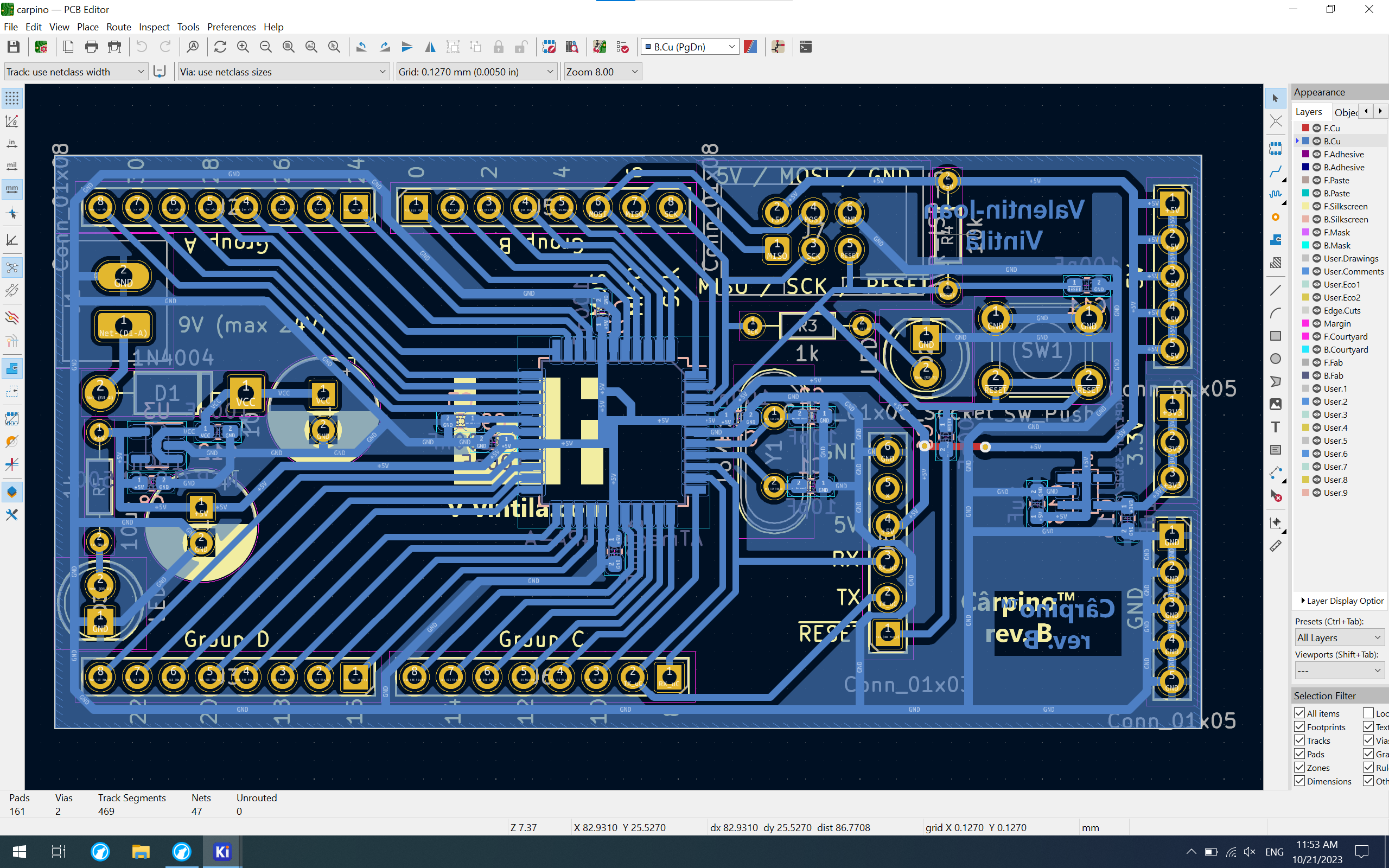
The PCB design (in KiCad)
Important considerations#
A few considerations were taken into account:
-
Every decoupling capacitor should be near the part that requires power;
-
As it was already mentioned above, the crystal should be in very close proximity to the microcontroller itself;
-
GPIO pins (or header pins) should be easily accessible.
All of these allowed for a great final result!
License#
As you can tell, I've completely open-sourced the board's circuit design. However, I do ask that you keep the name of the board and give me credit whenever you use the design.